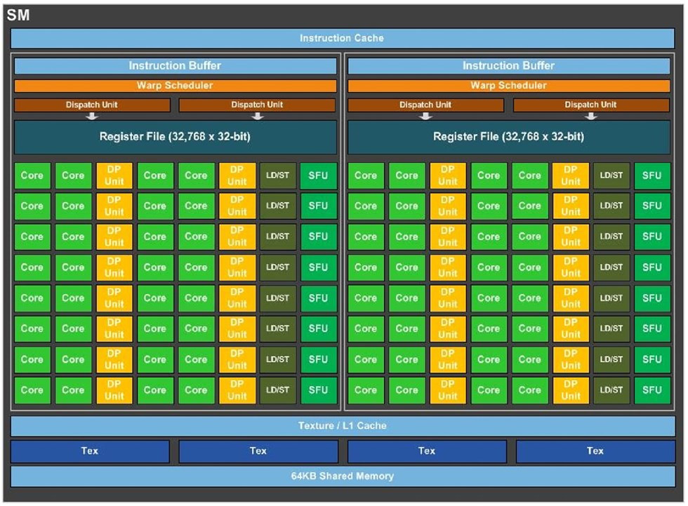
At its most top-level hierarchy, the GP100 is structured much like other NVIDIA GPUs, with the exception of two key interfaces - bus and memory. A PCI-Express gen 3.0 x16 host interface connects the GPU to your system, the GigaThread Engine distributes workload between six graphics processing clusters (GPCs). Eight memory controllers make up the 4096-bit wide HBM2 memory interface, and a new "High-speed Hub" component, wires out four NVLink ports. At this point it's not known if each port has a throughput of 80 GB/s (per-direction), or all four ports put together.

from techPowerUp! http://ift.tt/1RQpJ9W
via Techpowerup is my favorite place to get more review and the computer hardware part review, the review and the news is just so good, i really recommend you to visit the original page to read the full story about what the news beast and what the site talking about, enjoy the computer hardware part information online, visa techpowerup, i hope someday i will easily buying the new list item on the review list, just to make very beast computer rig, to encode the x264, that will kicking some ass... be ready
Post a Comment
This blog needed you to understand the word spam - never spam on this blog, although i will not moderate all of it, but you will learn it yourself, educate yourself